
BlackBerry Outages Shake User Confidence
Games |
2026-01-03 00:56:03
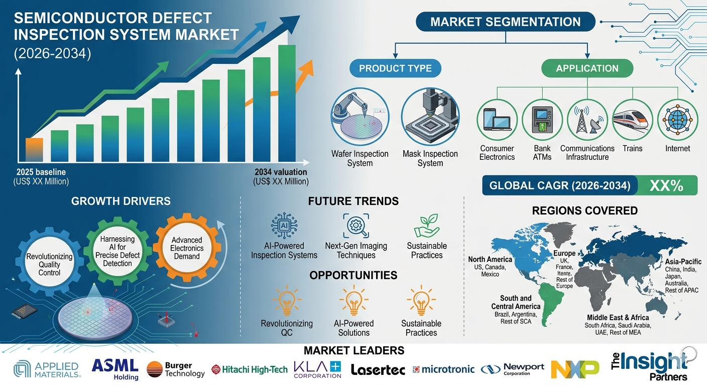
The semiconductor manufacturing ecosystem is evolving rapidly as chip producers develop increasingly advanced integrated circuits designed to support emerging technologies such as artificial intelligence, cloud computing, high-performance computing, and autonomous mobility systems. Semiconductor fabrication processes involve numerous highly precise stages, including lithography, deposition, etching, and packaging. At such microscopic scales, even the smallest contamination or structural irregularity can significantly affect device functionality and reduce manufacturing yields. As chip architectures become more sophisticated and miniaturized, maintaining strict quality control throughout the fabrication process has become a major priority for semiconductor manufacturers.
Advanced inspection technologies are essential for ensuring semiconductor production accuracy and reliability. Semiconductor fabrication facilities rely on highly sophisticated systems capable of detecting microscopic defects on wafers during different stages of manufacturing. These inspection platforms integrate optical imaging, electron beam inspection, and advanced analytics to identify contamination, pattern deviations, and structural flaws. As semiconductor devices continue to shrink in size while increasing in complexity, defect inspection technologies have become critical tools for improving production efficiency and maintaining high-quality standards across fabrication plants.
The Semiconductor Defect Inspection System Market in North America is experiencing steady expansion as semiconductor manufacturers strengthen their production capabilities and invest in advanced fabrication technologies. The Semiconductor Defect Inspection System Market Trends is gaining momentum due to the growing demand for high-performance semiconductor devices used in artificial intelligence, cloud data centers, advanced automotive electronics, and next-generation communication systems. Increasing investments in semiconductor fabrication facilities, along with government initiatives supporting domestic semiconductor production, are further accelerating the adoption of defect inspection technologies throughout the region.
Download Sample PDF Copy of this Report:
https://www.theinsightpartners.com/sample/TIPRE00017006
Expansion of Semiconductor Manufacturing Facilities
One of the major drivers supporting the adoption of semiconductor defect inspection systems in North America is the ongoing expansion of semiconductor manufacturing infrastructure. Governments and private technology companies are making substantial investments to strengthen local semiconductor production capacity and improve supply chain resilience.
New fabrication plants require highly advanced inspection technologies that can monitor wafer production across multiple manufacturing stages. These systems enable manufacturers to identify defects during lithography, deposition, and etching processes. Early defect detection helps semiconductor manufacturers prevent costly production losses and improve overall wafer yield rates.
Rising Demand for Artificial Intelligence and Data Center Processors
North America continues to be a leading hub for artificial intelligence innovation and cloud computing infrastructure. The rapid expansion of AI-driven applications, machine learning platforms, and hyperscale data centers is generating strong demand for high-performance semiconductor processors.
Manufacturers producing these advanced processors must ensure extremely precise fabrication standards. Semiconductor defect inspection systems allow engineers to detect microscopic wafer defects that could affect chip reliability or performance. As investments in artificial intelligence infrastructure and cloud computing platforms increase, the need for sophisticated inspection technologies will continue to grow.
Growth of Automotive Electronics and Electric Mobility
The automotive sector is rapidly adopting semiconductor technologies to support electric vehicles, connected mobility solutions, and autonomous driving systems. Modern vehicles rely heavily on semiconductor devices for sensor integration, battery management systems, infotainment platforms, and driver assistance technologies.
Because automotive semiconductor components must meet strict reliability and safety requirements, manufacturers depend on defect inspection technologies to ensure high-quality production. Inspection systems help identify structural defects during wafer fabrication that could compromise semiconductor performance in demanding automotive environments.
The continued expansion of electric mobility and intelligent transportation systems is therefore contributing significantly to the demand for semiconductor inspection technologies.
Miniaturization of Semiconductor Devices
The semiconductor industry is continuously advancing toward smaller process nodes to improve device performance and energy efficiency. As chip architectures become more compact and densely integrated, detecting manufacturing defects becomes increasingly difficult.
Modern defect inspection systems provide ultra-high-resolution imaging capabilities that allow engineers to identify nanoscale imperfections during wafer processing. These advanced technologies enable semiconductor manufacturers to maintain strict quality standards even as fabrication processes become more complex. The trend toward smaller semiconductor geometries is therefore a major factor driving the adoption of advanced inspection solutions.
Technological Advancements Improving Inspection Accuracy
Continuous technological innovation is significantly improving the performance of semiconductor defect inspection systems. Modern inspection platforms integrate high-speed optical scanning technologies, electron beam inspection, and artificial intelligence-based analytics to enhance detection accuracy.
Machine learning algorithms are increasingly used to analyze inspection data and automatically classify defects, enabling manufacturers to identify recurring process issues quickly. These intelligent inspection systems improve process control, reduce manufacturing downtime, and optimize production efficiency across semiconductor fabrication facilities.
Automation and real-time monitoring capabilities are also helping semiconductor manufacturers implement more efficient quality management processes.
Competitive Landscape and Key Players
The semiconductor defect inspection system industry includes several major global technology companies specializing in semiconductor manufacturing equipment and process control technologies. These companies are investing heavily in research and development to enhance inspection performance and support next-generation semiconductor fabrication.
Key players operating in this industry include:
KLA Corporation
Applied Materials Inc.
ASML Holding N.V.
Hitachi High-Tech Corporation
Onto Innovation Inc.
Camtek Ltd.
Lasertec Corporation
SCREEN Semiconductor Solutions
Advantest Corporation
Toray Engineering Co., Ltd.
These organizations continue to introduce innovative inspection technologies designed to improve wafer yield, enhance defect detection capabilities, and support advanced semiconductor manufacturing processes.
Future Outlook
The North American semiconductor defect inspection technology industry is expected to experience strong growth through 2034 as semiconductor demand continues to expand across multiple technology sectors. Increasing investments in semiconductor fabrication plants, growing adoption of artificial intelligence technologies, and rising demand for semiconductor devices in automotive and industrial applications will continue to support industry growth.
Advancements in artificial intelligence-based inspection systems, real-time process monitoring tools, and high-resolution imaging technologies will further enhance defect detection capabilities. As semiconductor manufacturing processes become more complex, inspection technologies will remain essential for maintaining production quality and ensuring reliable semiconductor device performance.
About Us
The Insight Partners is a leading global market research and consulting firm that provides in-depth analysis and strategic insights across various industry sectors. Our research reports offer comprehensive coverage of industry trends, technological developments, competitive landscapes, and growth opportunities, enabling organizations to make informed business decisions and achieve sustainable growth.
Contact Us
The Insight Partners
Email: sales@theinsightpartners.com
Phone: +1-646-491-9876
Website: https://www.theinsightpartners.com
Embedded Computing Market Share, Trends, and Growth Opportunity
Digital Twin Technology MarketShare, Trends, and Growth Opportunity